


White paper: Connector Related PIM
A Collaborative Research Programme Between:
Hughes Electronics Ltd and London Southbank University (LSBU)
Introduction
Co-axial cables deployed in the terrestrial infrastructure of Cellular Telecommunications provide an extremely efficient method of transmitting high frequency signals over recommended distances of up to 150 metres [1]. Signals are disturbed and problems occur however at the point where two cables are joined together, referred to as the Signal Transition Point (STP). According to Kaelus, one of the industry’s leading test equipment suppliers, jumper cables make a very significant (up to 42%) contribution to Passive Inter Modulation (PIM).
The real problem however, and the reason that jumper cables have been the recipient of such bad press is not the cable component of the jumper cable, but the connector serving the Signal Transition Point (STP) and terminating the (jumper) cable [2]. The shorter the jumper cable the greater the “connector effect” so counter to popular belief shorter jumper cables will generally make PIM worse not better.
Since connectors make a significant contribution to PIM, they have a pivotal role in reducing PIM. Extensive issues directly and indirectly responsible for PIM and other transmission problems are generated at the STP, where a signal transits from one component to another, e.g. cable to connector or connector to connector. At such transition points, small separations occur causing a capacitive coupling triggering distorted linear, non-linear and ‘ghost’ signals. The phenomenon is exacerbated by multiple micro-transition points in metal connector fabrication caused by the use of discrete metal components in transmission paths and the susceptibility of metal itself to electromagnetic interference (EMI), (the return transmission path is effectively formed of the metal outer body). 7/16 connectors are particularly vulnerable.
Long Term Evolution (LTE), especially fourth and proposed fifth generation networks are far more vulnerable to PIM and other signalling problems than any protocol that has gone before. Signal to Noise Ratio (SNR), not part of the PIM measurement but an important factor in the effect of PIM, is also far more sensitive to passive transmission problems. Putting this into perspective 4G requires 30 times greater SNR than 2 or 3G [3]. Higher frequency allocations and closer frequency layering combined with higher density data encryption and increased electrical radiations from the number of multiple frequency connections (up to 16) carried in limited space, all create the perfect storm for Network operators in the fight for Network reliability and consequent client fidelity.
This paper analyses the root cause and effect of disturbances caused by metal connectors, recognises the effects of metal fabrication induced transmission inefficiencies in connector related PIM and subsequently proposes a cogent and practical alternative. The WaveWay™ offers a coalesced structure of composite and metal materials in combination with unique design concepts to solve the problems of next generation networks.
Connector Related Sources of PIM
Metal connectors are the focal point for PIM in copper channels, they both generate PIM and receive and forward PIM from other sources including:
Connector Based PIM: PIM generated within the metal connector.
Channel Based PIM: PIM generated by a channel connector (or other component) and received and forwarded to the next part of the Channel by the metal connector.
Cross Channel PIM: PIM generated by another cable channel, radiated to and received by the metal connector and forwarded to the next part of the Channel.
Alien PIM: PIM generated by alien electromagnetic/environmental fields such as those created by motors or rusty metal objects surrounding the system and picked up by the metal connector.
The Metal Effect and the 7/16 Interface
Metal makes for a robust connector but is vulnerable to many impairments which cause PIM. All metal connectors are subject to the same vulnerabilities but none more so than 7/16 connectors in prolific use in Cellular Base Stations around the world. For this reason we use the 7/16 connector as our subject metal connector for comparison purposes.
Connector Based PIM – ‘Signals travel via skin effect, they require smooth undisturbed pathways, cuts, scratches, abrasions, sharp edges and corrosion create signal disturbances’.
As frequency increase AC current moves toward the outside of a conductor, this current “crowding” is called the skin effect. Figure 1 shows the cross-section of a single conductor in free space carrying a high-frequency current. If this was a DC current the current density, displayed as varying colours, would be the same throughout. The crowding phenomenon (skin effect) is indicated by the red and orange colours, where red forms the skin. Depth of penetration is defined as the distance from the outer surface to the point where the current density has fallen to 1/e of the outer surface current density. For copper, this depth is;
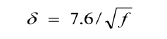
Where, f is in Megahertz and depth is in cm.
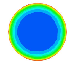 Figure 1 - Current crowds the outer surface of the conductor at high frequency.
A 1 GHz signal requires only 2 μm of skin depth thorough which to travel, a 2GHz signal only 1.4 μm and higher frequencies even less [4]. It is easy to see why a scratch of only 1 μm will have a deleterious effect on signal quality. The skin depth necessary for signal transit over a metal connector is usually provided by surface area treatment or ‘plating’ which is extremely vulnerable to abrasions but wholly necessary to mitigate corrosion of the underlying metal construction. If the underlying construction is bared by abrasions or flaking of the surface treatment PIM will increase through corrosion (which rings the death knell of communication signals in any event)
The problem for metal connectors occurs because the outer body and coupling mechanism is electrically connected to its outer contact. The exterior surfaces function not only as a coupling mechanism (to mate with other connectors) but as a return transmission path and also as an electromagnetic shield.
In its capacity as a coupling mechanism the connector outer body is subject to the normal rigours of installation including torque wrenching which frequently results in cuts, scratches and abrasions. Such physical damage is not compatible with its function as a return transmission path, it disturbs the signal and generates PIM. Corrosion, a by-product of physical damage, causes more PIM and other signal distortions. Regardless of physical damage the usual tri-metal (Cu-Sn-Zn alloy) plating applied in an attempt to delay corrosion is in itself corrosive, so given time corrosion based PIM seems in effect to be designed into the system.
Sharp edges of screw threads in the metal coupling nut (also acting as return path) distort RF transmissions too, adding to PIM. Figure 2 shows typical examples of damage connector surfaces sustain.
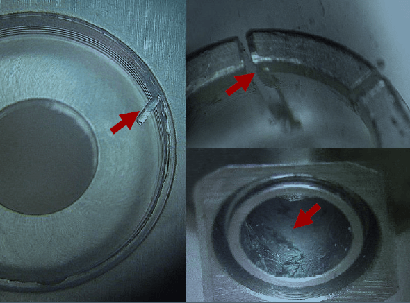
Figure 2 – Examples of typical connector surface damage including scratches, corrosion, metal flaking and damaged thread.
Connector Based PIM – ‘Separations in signal pathways cause signal phase shift, capacitive couplings, ‘ghost’ signals, and harmonic and non-linear transmissions’ [5]
Originating in the 1960’s the 7/16 connector was not designed for the demands now made of it. The connective interface is relatively poorly conceived, it started life with a slotted outer contact (fortunately that has now been replaced by a solid contact) but still only the leading edges of the inner and outer contact areas are designed to 'touch fit'. Astonishingly the standard allows for up to 1mm tolerance fit on some dimensions [6]. It is not surprising therefore to discover that different connector manufacturers’ parts vary; different dimensions and shapes may be seen between outer conductors, centre conductors and lengths etc. These uncertainties cause small separations in STP’s (the points where signals transit from one discrete component to another) causing electrical discharges. ‘Leaked RF’, capacitive couplings, ‘ghost’, harmonic and non-linear transmissions ensue, such connectivity issues lead to diminished SNR , signal phase shift and other non-trivial PIM distortions and signal quality issues. Moreover 7/16 internal signal transmission paths, in common with almost all metal connectors, are made up of multiple electrically conjoined and interacting metal parts throughout the connector, in effect macro ‘transition points’, effectively multiplying the issues by the number of transition points involved (generally a factor of 4).
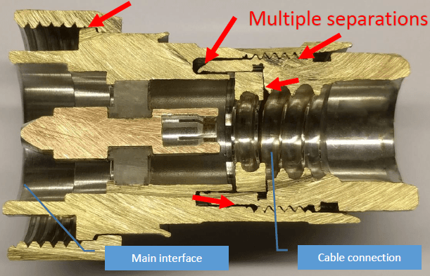
Figure 3 – Cross section of typical 7/16 connector showing component separations.
Sharp corners, another inherent design feature of metal connectors, radiate RF too. Each reflection and radiation provokes a further loss and mismatch of RF energy to the antennae (in fact this measured mismatch is a very good indication of connector based losses).
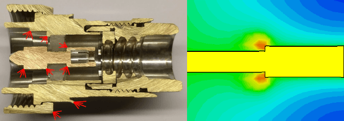
Figure 4 – On the left - cross section of typical 7/16 connector showing examples of radiative corners. On the right - simulation of e-field (electric field) radiation from sharp corners.
Confusingly for those charged with system efficiency it is also possible for a signal to distort through a separation which induces a phase change only to change back at the next separation and appear perfectly linear (a linear distortion) [7] . Such signals may appear normal on a PIM test but may be nothing more than undesired signal ‘noise’.
Connector Based PIM – ‘RF signals are extremely vulnerable; mixed materials and deformation of the structure within which they travel is an inadequate solution to a poorly conceived transmission path’.
Separations are the reason that high torque (25Nm) is recommended for 7/16 connectors. The torque is an attempt to “squash” or homogenise discrete metal components in the transmission path in an attempt to create a passably unseparated signal conduit with tolerably low resistance.But high torque changes the form of the metal which can cause the tri-metal plating (in which the skin effect transmission travels) to crack and flake generating PIM and other fatal disturbance problems. Under torqueing provides an equally poor outcome for PIM as any rigger skilled in the art will testify, separations do not close sufficiently resulting in the transmission problems already described.
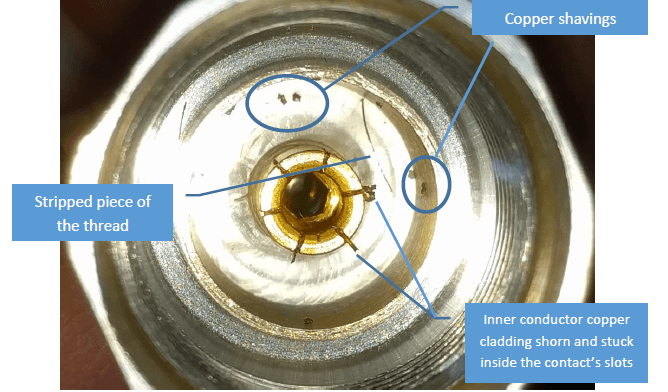
Figure 5 – Rear view of typical 7/16 connector showing PIM source effects of a single mating using recommended torque.
In reality creating the desired torque in hostile environs and confined spaces such as antennae poles occupying up to 16 other cables can be difficult to impossible. Contact resistances and insertion losses quoted by manufacturers using fully torqued ideally matched components in the laboratory are therefore rarely, if ever actually achieved in the field.
Whilst high torque can to some degree reconcile separations at the frontal transition point in the critical forward path between male and female contacts it does not help at the rearward (cable side) transition point. Separations where the cable meets the rearward connector contact are usually reconciled by resistive soldering which generates its own problems. Even the best technicians in the world cannot provide a solder joint that is not disruptive to RF signal linearity; a little too much flux applied or contained in the solder (or if the flux is not completely evaporated) will cause the joint to crumble in time causing PIM. On the other hand if too little flux is applied the resulting joint will be a cold solder joint and vulnerable to cracks resulting in the same problems. Consequently it is a common phenomenon that jumper leads which have passed a PIM test with flying colours at the point of manufacture or installation can fail miserably two weeks later. Added to this, poor quality (or the wrong type) solder may also contain impurities which generates even more PIM.
Additionally, imperfect material matches between the solder and pin/contact/cable conductor are a direct source of reflections, distortions and signal nonlinearity [8], [9].
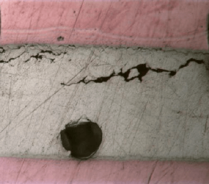
Figure 6 – Solder joint interconnection cross-section showing typical distortive imperfections.
Connector Based PIM – ‘Impedance mismatches cause reflections and low SNR’ [7]
Mismatched impedance, whilst not a recognised source of PIM, can increase the effect of PIM. Impedance mismatches cause reflections, each signal reflected diminishes SNR. The lower the amount of expected desired RF energy an antennae receives, the less efficient it becomes and the greater the effect of undesired ‘noise’. Whilst frequencies of < 1000MHz are fairly tolerant to impedance mismatches the consequences of higher frequency mismatches become much more severe. Next generation networks are particularly vulnerable, in fact every ohm counts.
In addition, if the reflected signals become “trapped” in improperly or poorly grounded cables they manifest as unwanted ‘self-interference,’ growing to become destructive and egressing through metal connections to other channels in the near vicinity via the ‘Crosstalk’ effect (see alien PIM).
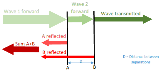
Figure 7 –Each separation provokes a distortive signal modulation and provokes reflections which reduces SNR.
NB. It is worthy of note that none of the market leading metal connectors tested in this research provided satisfactory impedance in the frequencies of >1200MHz. Moreover most (if not all) PIM test equipment presumes 50 ohm impedance; actual impedance or VSWR of the device under test is not calculated in PIM “value” expressed (see a word about PIM testing) .
Channel based PIM – Cable movement generates ‘Microphonics’
Slight movement of cables (a frequent occurrence) can result in tremors and resonances being introduced into cable channels, these resonances develop as microphonics [10]. On a simple physical level microphonic reverberations can loosen the connection at the important signal transit area, on an electrical level the reverberations generate pulses or spikes to the detriment of the signal. Metal connectors are ready receivers and transmitters of unwanted microphonic disturbances; they will happily pass (the microphonics) along to the next part of the transmission channel, intensifying as they propagate. Such microphonic disturbances are propagated as cable ‘noise’, further reducing the effective bandwidth and contributing to signal losses/reduced SNR and adding to the PIM effect.
Alien PIM – ‘Cross Channel and Environmental Interference’
Coaxial screening provides a defensive “shield” to RF signals, blocking both ‘inbound’ and ‘outbound’ electromagnetic radiations and disturbances. Formed as a co-axial metal layer to a central contact (carrying the forward path) the shield also forms and acts as an outer contact (carrying the return path). This axial outer formation forms a very effective RF barrier in a solid unbroken layer such as in conventional corrugated cable [4].
But a channel shield is only as good as its weakest point, in this case the metal connector whose outer contact is formed of a number of discrete metal parts and consequent micro separations from which RF willingly radiates. Moreover being metal and an electrically connected return path it is susceptible to egress and radiations from other connections or other alien electro-magnetic interference (EMI). It therefore provides a ready conduit for interference into its channel return path.
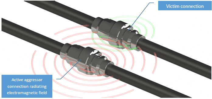
Figure 8 – Showing energy transfer between two adjacent 7/16 channels
When cables are improperly grounded as may be the case in packed antennae poles (where there may simply not be enough room) the received interference is trapped within the cable, adding to reflections already present and growing to become an aggressive source of irresistible “noise”, generating PIM and diminishing available bandwidth.
The effects of this phenomenon are compounded by (the channels’) containment in metal antennae poles which act as an overall screen to up to 16 other cables often transmitting at different frequencies and radiating high frequency RF to neighbouring connections within the pole. Moreover the connectors tend to sit in very close proximity at access windows, as shown in Figure 9 below, and if an exposed metal connector touches another the effects on PIM and dropped signals provide very poor outcomes.
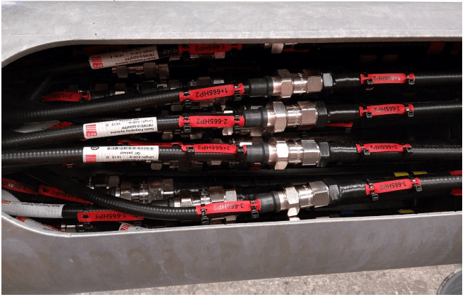
Figure 9 – View of the RF feeder cables inside of the antennae pole (courtesy of Hutchinson Engineering Widnes U.K).
A similar phenomenon is experienced when metal connectors are exposed to other nearby sources of EMI such as motors, radios and electrical equipment; all of this interference is passed into the cable channel via the connector for onward transmission augmenting PIM and reducing SNR.
Alien PIM – Temperature variations are a long term destructive force for metal connections
Temperatures of up to 56.7 °C (134 °F) have been recorded in places such as North America; temperatures hot enough to fry an egg on the pavement are regularly reported by popular media around the world. Much lower ambient temperatures however can have a marked effect on PIM because metal has a high thermal mass/heat capacity [9].
Initially the effect of heat on metal connectors can be beneficial, the metal expands and the discrete metal parts of the connector are compressed, reducing separations and naturally forming a more benign transit path for signal transmission. As the metal cools however, separations become greater, significantly increasing PIM by up to 10dB. This phenomenon is compounded by continuous heating and cooling which has the effect of exacerbating separations through loosening of torqued mating threads and electrical line contacts. Solder or welding joints used in factory assembly of jumper cables suffer too, the material is fractured causing further detrimental separations during temperature cycling.
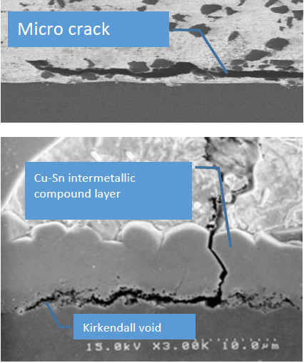
Figure 10 – Magnified sectional views of voids and cracks in solder joints due to thermal cycling.
The adverse effects of temperature can be visualised from the body temperature and corresponding
PIM variations of a Device Under Test (DUT) over time after exposing it to a 100°C heat source for 1
minute, shown in Figure 11.
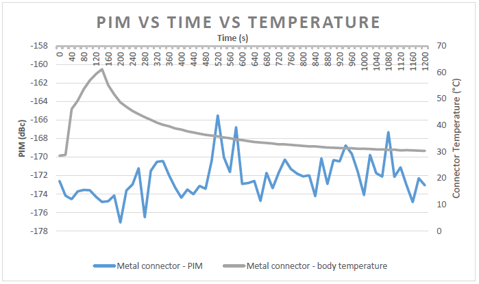
Figure 11 – PIM test results for metal connector exposed to 100°C heat source for 1min
Finding a better way
A leading edge development group formed of technical experts from Hughes Electronics took on the task of designing a connector that would diminish PIM by reducing the problems caused by connections - “The Better Way”. The Hughes team was joined and assisted by researchers at the Biomedical and communications (BiMEC) research group at London Southbank University.
The group found that basic design principles of connectors under test, in common with other metal connectors were flawed in that, in combination with its function as a return path, the outer body is required to perform too many functions. (i) As a coupling mechanism to other connectors it is prone to damage (causing PIM), (ii) as a return path it’s design is distortive and disruptive to signals (causing PIM and distortions) and (iii) as an exposed screen or shield it is vulnerable and susceptible to Alien PIM.
Problems were also found in the forward path and it was noted that difficulties mostly centre on the singular choice of metal as a construction material combined with poor design choices.
The WaveWay™ Connector
The first principle for the development group was to define a connector that reduced connector related PIM source problems in a commercially viable way. It was decided that the innovation should be legacy compatible to existing 7/16 connectors, easy to fit in the field, deployable in existing infrastructures (including legacy cables) and of course commercially viable.
The key to the performance conundrum appeared to lay in separating and isolating the connector functions, designing a small number of parts with single dedicated functions doing their job well, rather than an assortment of multipart pieces - jacks of all trades but masters of none.
Prime considerations were to isolate the outer contact/screen from the outside world and to improve signal transit paths and mating areas by reducing separations.
Features and Benefits of the WaveWay™ connector
Connector Based PIM– Cuts, scratches, abrasions, sharp edges and corrosion designed out.
It was clear that the development team were powerless to stop damage happening, the outer body of a connector would always be subject to degradation. Isolating the damage from the transmission path however would effectively remove PIM from this source. The preferred method of isolation was to change the material of the outer body in order to disconnect it from the outer contact. The method also had the benefit of isolating the outer contact, protecting it from Alien Source PIM including cross channel PIM and reducing it to zero. An additional benefit was to disconnect the coupling mechanism from the signal transit path providing a much improved signal pathway. The initial material of choice was a mix of glass fibre filled Acrylonitrile Butadiene Styrene (ABS) and polycarbonate (PC), an extremely durable and flame retardant composite with a high tolerance to temperature extremes and UV as well as being non-corrosive. Alternative polyethylene (PE) based materials were also investigated but discounted.
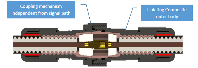
Figure 12 – cross sectional view of mated WaveWay™ connectors showcasing Isolating composite body and independent coupling mechanism.
Connector Based PIM –Separations in connector transmission paths and high torque to reconcile the problems they cause were designed out
The most effective method of dealing with separations was to remove them from the equation.
The WaveWay™ connector incorporates a one piece outer contact whose design is the inverse of the cable outer contact up to the point where it mates with its opposite gender. The single structure eradicates separations in the return transmission path and importantly because the structural form is exactly the inverse of the shape of the cable return path the symmetry of the signal is maintained in harmony and in phase with the cable up to the point of transit from one connector to another.
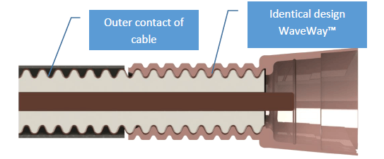
Figure 13 – Cross sectional view of Male WaveWay™ mated with cable showing synergistic design of signal transition area on return transmission path.
A unique conical coupling feature is incorporated at the forward connection area where one connector “mates” with another. Male and Female cones conjoined on outer to inner surface provide a 'sticky' interface with excellent mechanical alignment and electrical contact. The cone feature provides a very efficient low PIM Signal Transmission Point when coupled with other WaveWay™ connectors and provides the benefit of a compatible ' touch fit' legacy connection to all leading manufacturers’ 7/16 connectors irrespective of deviation from mean standard tolerance.
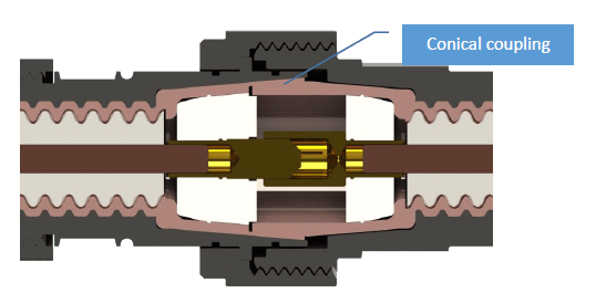
Figure 14 – Sectional view of Male and Female WaveWay™ connectors mated together via low torque, low resistance conical coupling feature.
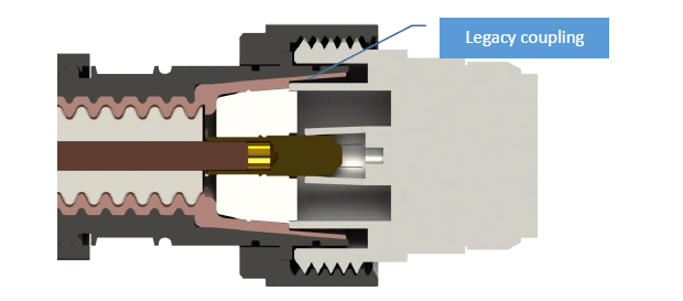
Figure 15 – Sectional view of Male WaveWay™ connector mated with 7/16 Female connector showing high torque touch fit legacy mating feature.
The conical mating area and the undulating design of the outer contact both rely on high surface area adhesion, not torque to provide (very) efficient signal transit areas. The reduction of separations and high surface area adhesion of the coupling mechanisms provide extremely stable Signal Transition Points with high resilience to impact, trauma, cable bending or reverse torsion.
Similar high contact surface adhesion at transit areas in the forward path was achieved through choice of materials and design. The material choice for the centre contact was a high quality Beryllium Copper material (Be Cu), a tensile metal with very high memory. The design is self-regulating, requiring no (signal) distorting solder, crimping or torque to provide improved signal transit. The inclusion of a non-conductive collet on the female contact in the original designs was later abandoned when the team discovered high surface area adhesion was maintained through 200+ mating cycles without the collet – deeming it unnecessary.
Radiative angles were reduced throughout the forward and return paths causing an increase in SNR.
Overall the WaveWay™ connector provides exceptionally reduced PIM from separation induced capacitive couplings, ‘ghost’ signals, harmonics and signal phase shift. The Synergistic undulations with the cable form provide an almost indestructible high surface area bond. No torque is required to affix the WaveWay™ therefore a hand terminable, a very low PIM, IP 68 rated Jumper cable can be fabricated in the field in minutes.
Channel based PIM –Microphonics
Microphonics in cable channels are a fact of life that no amount of cable securing can stop. Unlike metal, microphonic absorption in plastics and in particular ABS (which is a compound that includes rubber) is very high. Since the composite outer body of the WaveWay™ connector is part ABS and directly attached to the outer contact it absorbs and mitigates the effect of microphonics. The WaveWay™ also deploys a specially designed Ethylene Propylene Diene Monomer (EPDM) washer between the rear of the WaveWay™ and the cable outer conductor to buffer and absorb most microphonics before they arrive at the connector signal path itself. The benefit is that many microphonic disturbances are not passed to the signal transition area and importantly not passed through the connector into the next part of the transmission channel.
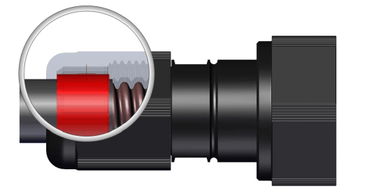
Figure 16 – Sectional detail view showing in red specially designed EPDM (M-class) microphonics buffer at the rear of the WaveWay™ connector
Alien PIM – Cross Channel and Environmental Interference
LTE and multiple frequency co-location bring new levels of complexity to cross channel interference caused by electrical discharges and radiations from metal connectors but provides the perfect environment for none conductive materials to demonstrate their superiority.
The tenet of the ‘crosstalk’ effect is that prevailing ‘aggressor’ channel emissions migrate to lesser ‘passive’ channels. Higher frequencies provoke more aggressive behaviour than lower power or less aggressive channels so the effect of RF migration and intermodulation will generally be more pronounced in constrained mixed frequency environments [10], [11].
Multi-frequency co-location increases the effect of cross channel interference, the WaveWay™ connector demonstrates its superiority in the environment however since contact areas and transmission paths are isolated by its composite outer body thus induced Cross Channel interference and PIM from other Alien sources are mitigated to virtually Zero.
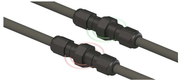
Figure 17 – Two WaveWay™ channels with reduced cross channel interference
Alien PIM – Thermal variations
The body of the WaveWay™ connector has much lower thermal mass than its metal equivalent. Since the outer contact is a one piece structure there are no separations that can be affected by heat one way or another.
No solder or welding process is used to affix the WaveWay™ to cable so distortions from thermal effect separations (and impurity effect) on those materials are also nullified.
The effect of heat on the WaveWay™ connector is far less severe than metal connectors. Figures 18 and 19 demonstrate PIM against temperature and time and connector body temp rise due to an RF signal against time, respectively. In the former it can be observed that the WaveWay™ outperforms typical metal connectors in both body temperature (20 difference in variation) providing a faster return to normal with less PIM variation and lower PIM across the time test.
In the latter Figure, the WaveWay™ demonstrates a steadier performance and lower temperature change in both tests over time than existing commercial metal connectors.
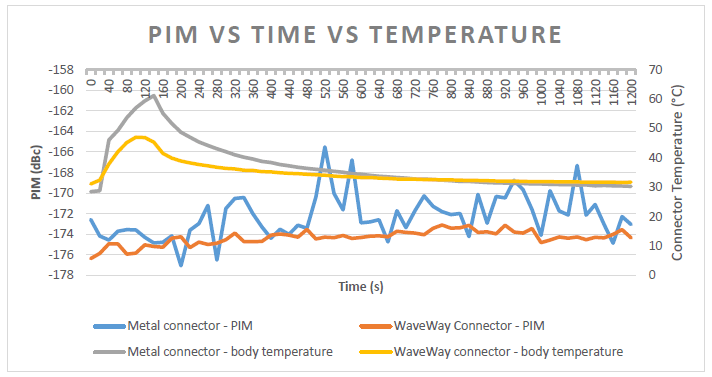
Figure 18 – Comparison of PIM test results for metal and WaveWay™ connectors exposed to 100°C heat source for 1min
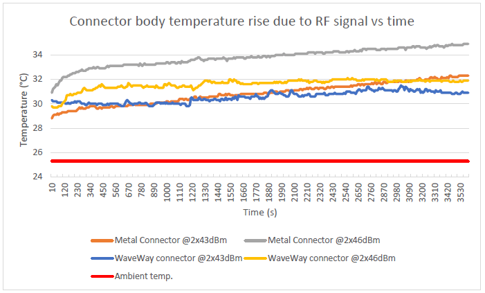
Figure 19 – Comparison of metal and WaveWay™ connectors’ temperature rise due to RF signal
The bar chart in figure 20 shows the comparison between the temperature changes of metal and WaveWay™ connectors in two different power scenarios. It can be seen that in both cases the WaveWay™ connector experiences less change with the respective temperature. Similar comparisons are pictured in figures 21 and 22, show that after both types of connectors were heated to 52°C, it takes less time for the WaveWay™ connector to reduce its temperature, and with an improved heat absorption and dissipation time, respectively.
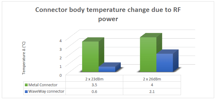
Figure 20 - Comparison of metal and WaveWay™ connectors’ temperature change due to RF signal
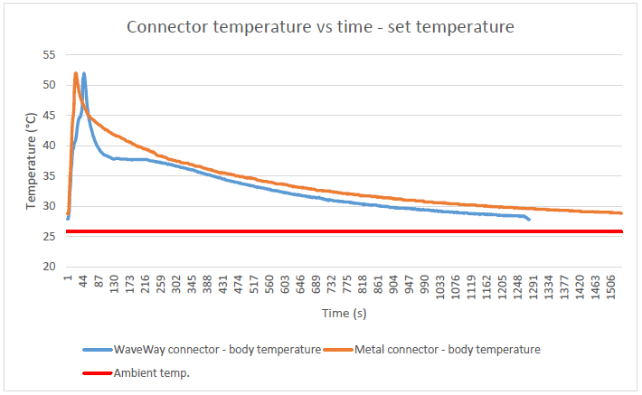
Figure 21 – Comparison of metal and WaveWay™ connectors’ temperature after heating the connectors to 52°C
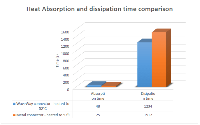
Figure 22 - Comparison of metal and WaveWay™ connectors’ heat absorption and dissipation time after heating the connectors to 52°C
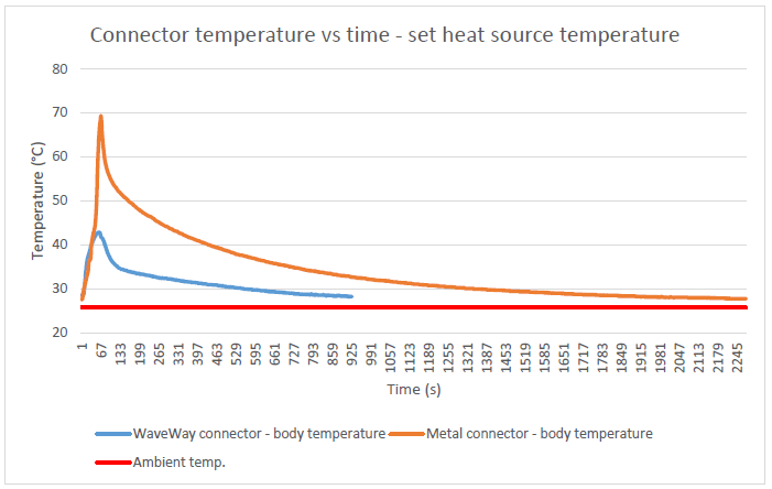
Figure 23 – Comparison of metal and WaveWay™ connectors’ temperature after exposing the connectors to 100°C for 1min.
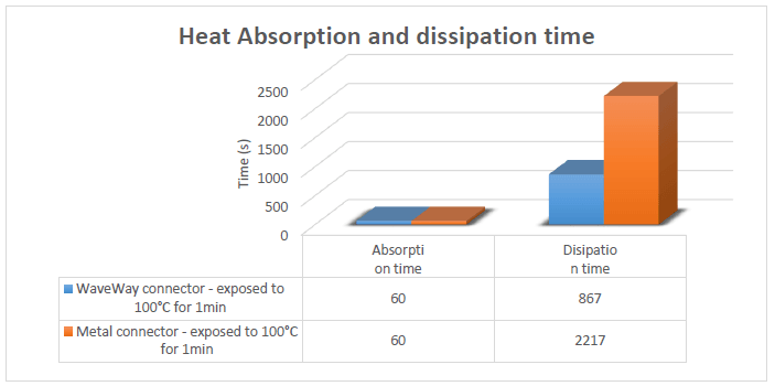
Figure 24 – Comparison of metal and WaveWay™ connectors’ heat absorption vs dissipation time after exposing the connectors to 100°C for 1min.
PIM Phase - a Novel approach to Improving Signal to Noise Ratio and PIM cancelation
As part of the work investigating the effect of separations in transmission paths the development team discovered that signal phase was vulnerable to change at separated points. The phase shift and associated reflections caused consequential corruption of the signal. It became clear during investigations that preserving phase throughout the transmission process from one component to another helps preserve the integrity of the signal and significantly improves SNR compared to the disturbed phase signal paths seen in conventional metal 7/16 connectors. The WaveWay™ design features were therefore optimised for use at the usual 800, 900, 1800, 2100 and 2600 MHz frequencies.
Additionally, frequency measurements showed that standard (jumper) cable lengths of 0.5 metre, 1 metre and multiples thereof did not provide optimal path lengths for the commonly used wavelengths and therefore contributed to phase shift and reflections. Adjusting cable lengths to sub-multiples of the operating wavelengths significantly mitigated the effect of phase shift and reflections thus improving SNR.
Other Connector Based losses – Impedance
Impedance, a calculation of the Voltage Standing Wave Ratio (VSWR) also known as the Variable Standing Wave Ratio is central to the RF energy, SNR, desired/ undesired signal equation. Poor impedance matching between Antennae and channel components such as connectors and cables cause reflections, each reflected sinusoid causes a co-related loss of RF energy to the Antennae and of course diminishes SNR.
Lost energy from reflections and radiations create an unbalancing of the system and reduce the RF available to the antennae [7] diminishing its transmission energy therefore increasing the effect of undesired energy.
The WaveWay™ development team had the benefit of knowing how critical impedance matching would be in the compacted layer environment of LTE; something the designers and specifiers of the 1960's could never have imagined. A great deal of thought therefore went into designing the WaveWay™ connector to produce a perfectly matched impedance of 50 ohm ±0.5 ohm throughout the critical 4G frequency ranges up to and including 2800 MHz The result is the best impedance matching in those frequencies of any connector tested (some of which had a 5 Ohm divergence to the nominal), far fewer reflections much improved SNR and antennae efficiency.
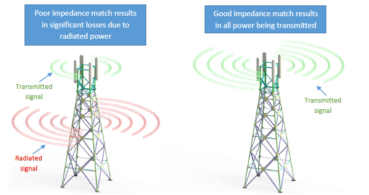
Figure 25 – Cell tower with poorly matched components (on the left) causing most of the signal to be lost or radiated. Cell tower with properly matched efficient transmission channel (on the right) – all power is transmitted through the antennas.
A word about PIM testing
LTE networks’ high order modulation methods have an innate low tolerance for interference or signal noise, it’s susceptibility to interference requires a much higher SNR. Acceptable levels of interference in 2G or 3G sites may be ruinous to an LTE deployment [3], accordingly LTE requires a much higher SNR to cope; 3G requires SNR of just 6dB to operate effectively, about 1/30th of that for optimal LTE performance.
Although limited in scope to non-Linearity of signals, PIM Testing and in particular a nominal PIM test result of less than -160 dBc* seems to have become the (false) Nirvana for the whole of the cellular industry. The assumption that a linear signal must be a “good” signal however is incorrect, whilst testing well for linearity a signal may have changed phase and distorted several times eventually moving back into phase carrying mostly distorted and useless “data noise”.
Such linear distortions generated by the culmination of reflections, insertion losses, capacitive couplings and other connector driven noise, i.e. a signal interfering with itself, are much harder to isolate than a single interference from an external source since they are generally back in phase and within frequency. A channel can provide a good PIM test but SNR and actual signal performance is actually very poor.
A good impedance match (predicated on VSWR measurement) between antennae and system is essential to achieve high SNR and maximum radiated power from the antennae. Returned signals from impedance mismatches and radiated RF unbalances the system, diminishes the power of the antennae and in turn enhances the effect of undesired frequency interference (PIM). Putting that into perspective each extra 10db of radiated power results in 3.16 greater distance of desired signal power radiated from the antennae. [7]
The resulting reflections and signal losses from a connectors’ divergence from 50 ohm will diminish SNR and the systems resilience to PIM so it is alarming that most PIM testers presume rather than calculate impedance. Whilst PIM measurements may be good information perhaps a debate must be had in respect of their veracity. A measurement of desired signals seems equally, if not more, important than measurements of linear signals [13] so dismissing real life impedance calculations and dislocating the two measurements seems a poor evaluation of system performance.
Other than the WaveWay™ connector none of the connectors tested posted an acceptable result in respect of impedance, it seems clear that the designers of 7/16 connectors of yesteryear could not have known of the demands LTE, 4G and proposed 5G would make on their creations but what is clear is that we should now take the VSWR/SNR equation as seriously, if not more so than PIM when measuring system efficacy.
The WaveWay™ connector outperforms and retards external interference by isolating the valuable RF it carries.
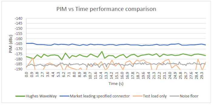
Figure 26 – Comparison of field terminable metal and WaveWay™ connectors’ PIM over time performance
Conclusion
Data demand grew 70% between 2012 and 2014 and as video streaming becomes universal the projections for 2019 are in the magnitude of 700% greater [14]. The increased amount of multi frequency equipment mounted on tower tops to satiate demand place a far greater burden on the backhaul connectors and other passive components that serve it.
Metal connectors are extremely robust but, given their vulnerabilities and 20th century design it seems difficult to make a case for them in 21st Century Networks.
Poor signal performance and by consequence poor customer fidelity costs aside, the cost/benefit equation of deploying metal connectors such as 7/16 to network operators and implementers seems implausibly high. Connector taping alone (in a mandatory but dubious attempt to ward off ingress and retard corrosion) costs stand at one rigger man day [15] for every antennae pole equipped with 16 cables.
Metal connectors radiate and egress energy or ‘talk’ to other channels and disempower the antennae increasing the effect of PIM. They demonstrate very poor SNR, poor heat tolerance, are susceptible to corrosion and difficult to assemble on site with any degree of consistent performance and reliability which degrades over time in any event with a net effect of decreasing SNR and increasing PIM.
By contrast the WaveWay™ facilitates a high performance field terminable, reliable connection via its patented one piece, solderless signal transition areas on forward and return paths. High surface adhesion provides exceptional SNR and resilience to PIM whilst the IP68 non-metal composite body design is indefinitely corrosion free, retards egress and is unsusceptible to cross channel and alien source PIM.
References
[1] CCNA Self-Study: CCNA Basics (CCNAB), Published Dec 16, 2002 by Cisco Press
[2] Rick Hartman, Measuring Passive IM of RF Cable Assemblies, Kaelus Inc., 2011, (www.kaelus.com)
[3] LTE Best Practices, Commscope, 2015, (www.commscope.com)
[4] HUBER+SUHNER RF CONNECTOR GUIDE 4th edition, 2007, (www.hubersuhner.com)
[5] Richard A. Thompson, The Physical Layer of Communications Systems, Artech House, 2006
[6] IEC 61169-4:2008(E), Radio-frequency connectors – Part 4: RF coaxial connectors with inner diameter of outer conductor 16 mm (0,63 in) with screw lock – Characteristic impedance 50 Ω (type 7-16)
[7] David Ballo, Hewlett Packard Network Analyser Basics
[8] Ray Butler, PIM Testing - Advanced wireless services emphasize the need for better PIM control, Commscope, 2014, (www.commscope.com)
[9] https://en.wikipedia.org/wiki/Intermodulation
[10] http://urgentcomm.com/mag/radio_importance_coaxial_cable
[11] D. W. P. Thomas, F. Leferink and H Bergsma, Practical Measure of Cable Coupling, 2009
[12] Purdue University, Prediction of passive intermodulation from coaxial connectors in microwave networks, January 2008
[13] S. Hienonen and A.V. Raisanen, Effect of load impedance on passive intermodulation measurements, 2004
[14] Global Market Broadband Update, Jan 2015
[15] Source: Qualitas UK